 en
en English
 Deutsch


If you need any help, please feel free to contact us
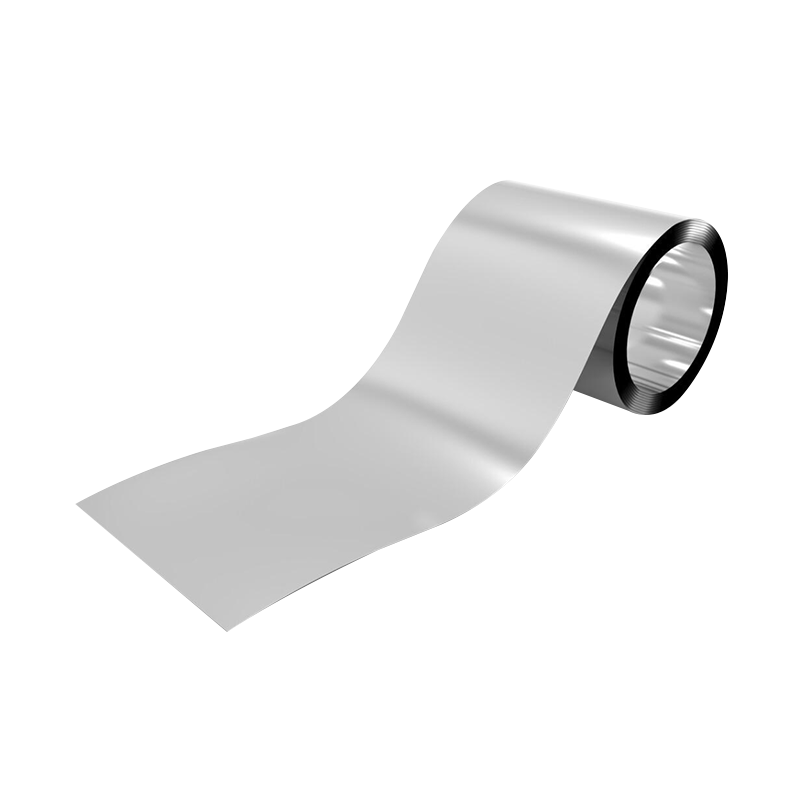
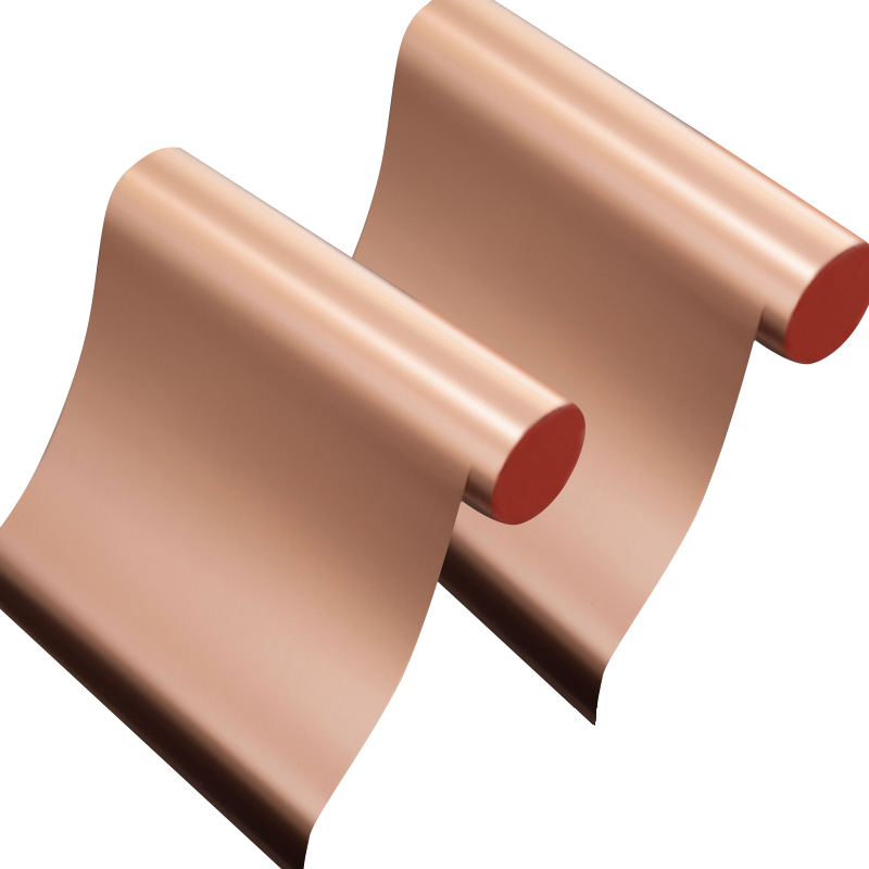
The Evolution of IC Lead Frame Technology and Its Impact on Semiconductor Packaging
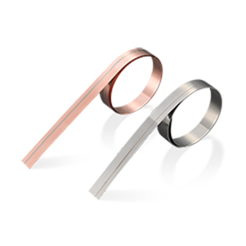
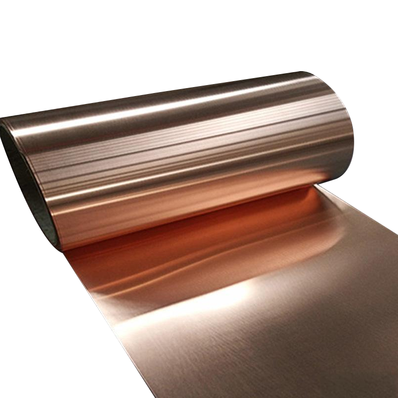
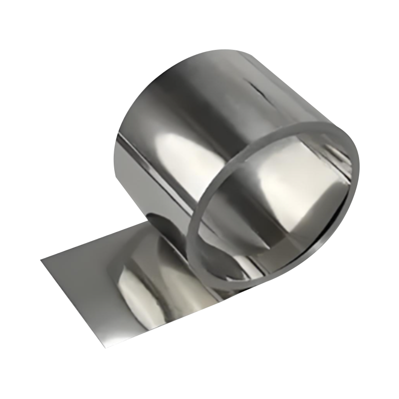
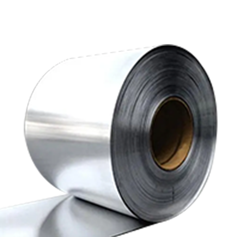
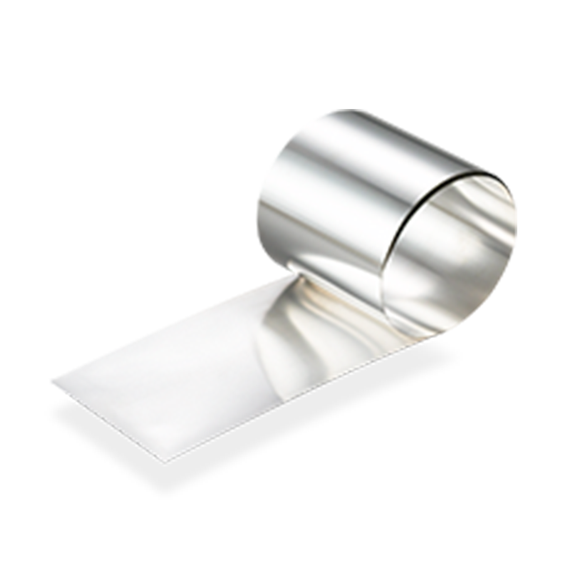
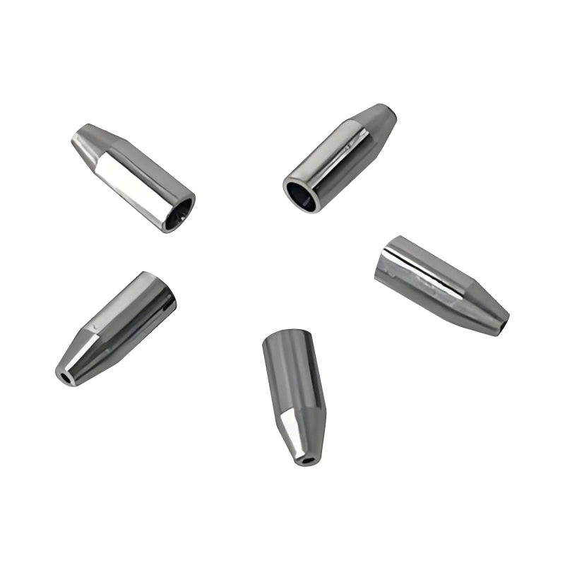
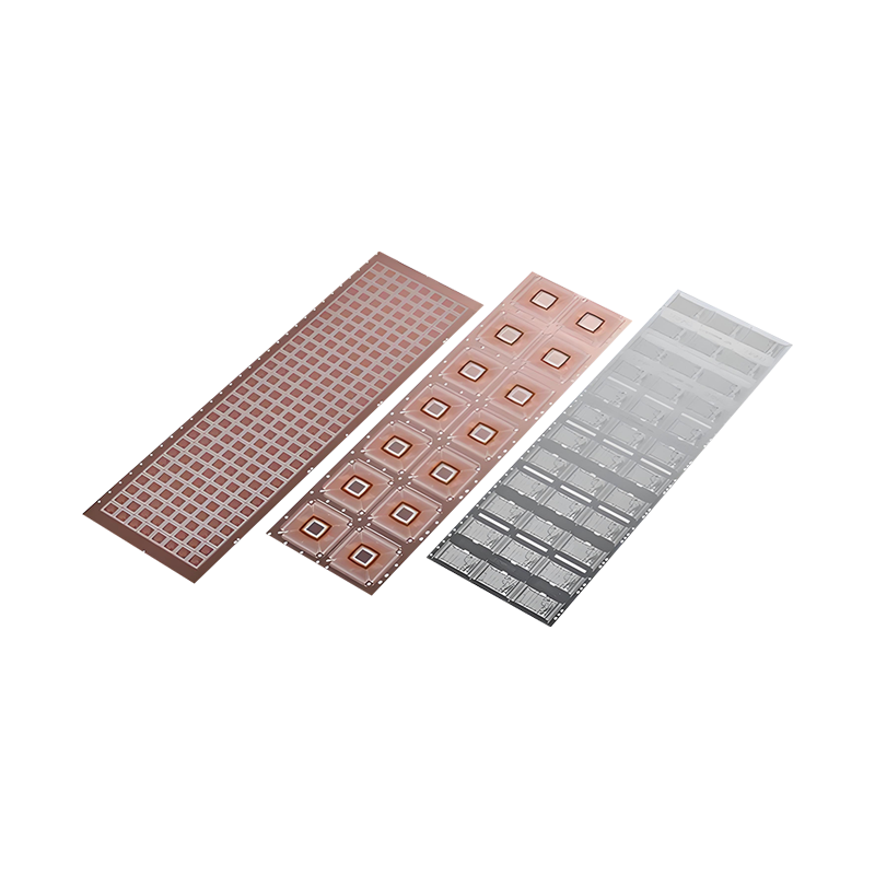
The journey of the IC lead frame has mirrored the rapid advancement of semiconductor packaging technologies over the past few decades. From the early days of through-hole mounting with dual in-line packages (DIP) to today’s ultra-compact chip-scale packages (CSP), lead frames have continuously evolved to meet the demands of miniaturization, performance, and reliability. Initially designed as simple metal frameworks to support and connect chips, modern IC lead frames now incorporate complex geometries, advanced materials, and precision surface treatments to handle high-speed signals and thermal loads in increasingly compact electronic systems.
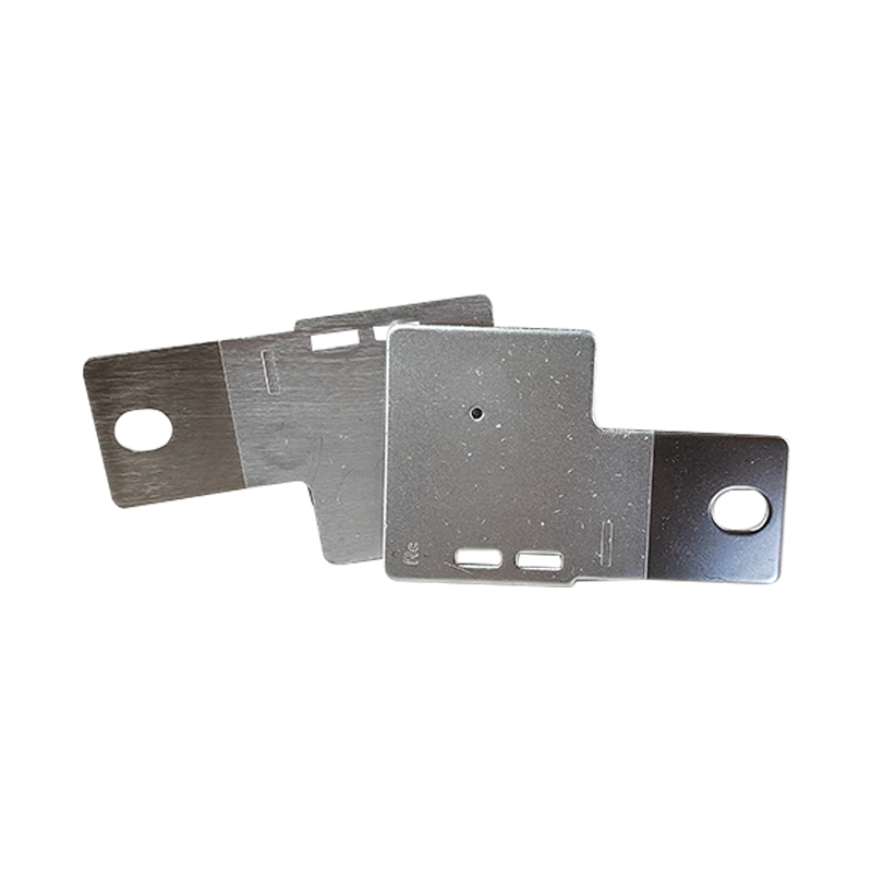
One of the earliest packaging formats that utilized lead frames was the DIP package, which dominated the industry during the 1970s and 1980s. These packages featured two parallel rows of pins and were suitable for printed circuit board (PCB) assembly using through-hole technology. However, as electronics began shrinking and performance expectations grew, new packaging styles such as Quad Flat Packages (QFP) emerged. These required finer lead spacing and better thermal dissipation, pushing the design limits of traditional IC lead frames and prompting innovations in etching and stamping techniques.
In the late 1990s and early 2000s, the rise of flip-chip and ball grid array (BGA) technologies introduced a shift away from wire bonding in some applications. Yet, for cost-sensitive and mid-range performance devices, IC lead frames remained central, especially in thin-profile packages like Thin Small Outline Packages (TSOP) and later in advanced formats such as Dual Flat No-leads (DFN) and Quad Flat No-leads (QFN). These newer designs not only reduced footprint but also improved electrical conductivity and thermal management—key considerations in mobile and automotive electronics.

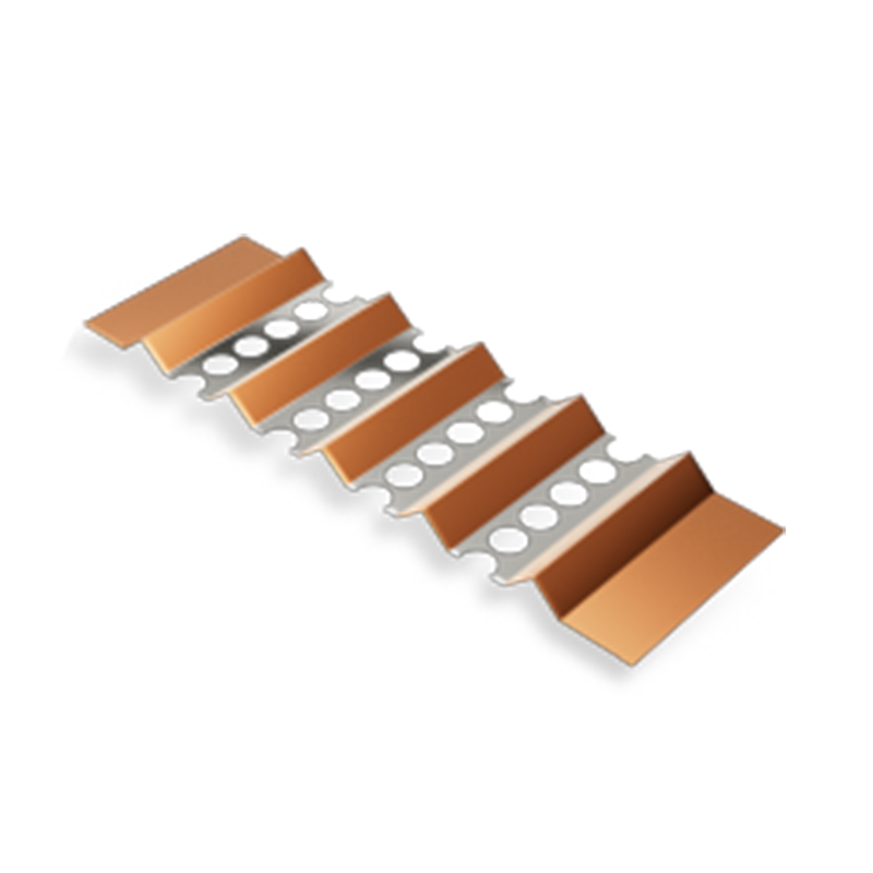
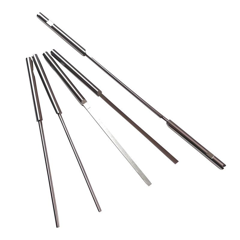
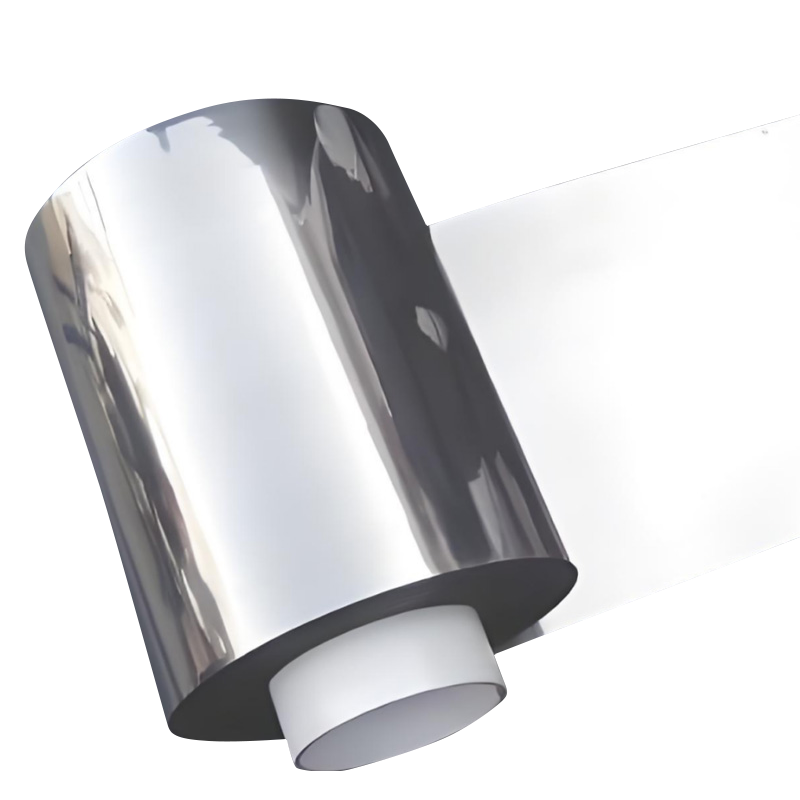
The development of high-density IC lead frames marked another major milestone in this evolution. As integrated circuits became more complex, so did the need for lead frames capable of accommodating hundreds of leads within a limited space. This led to the adoption of ultra-thin etching technologies and laser-cutting methods, allowing manufacturers to produce lead frames with micron-level accuracy. These advancements enabled finer pitch spacing and minimized signal interference, making them ideal for use in high-frequency communication modules and embedded systems.
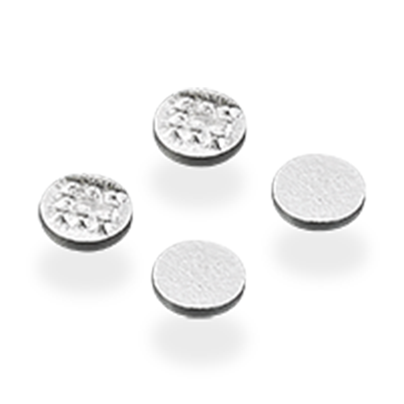
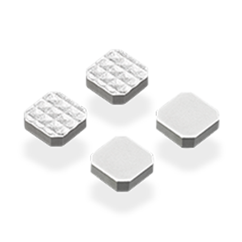
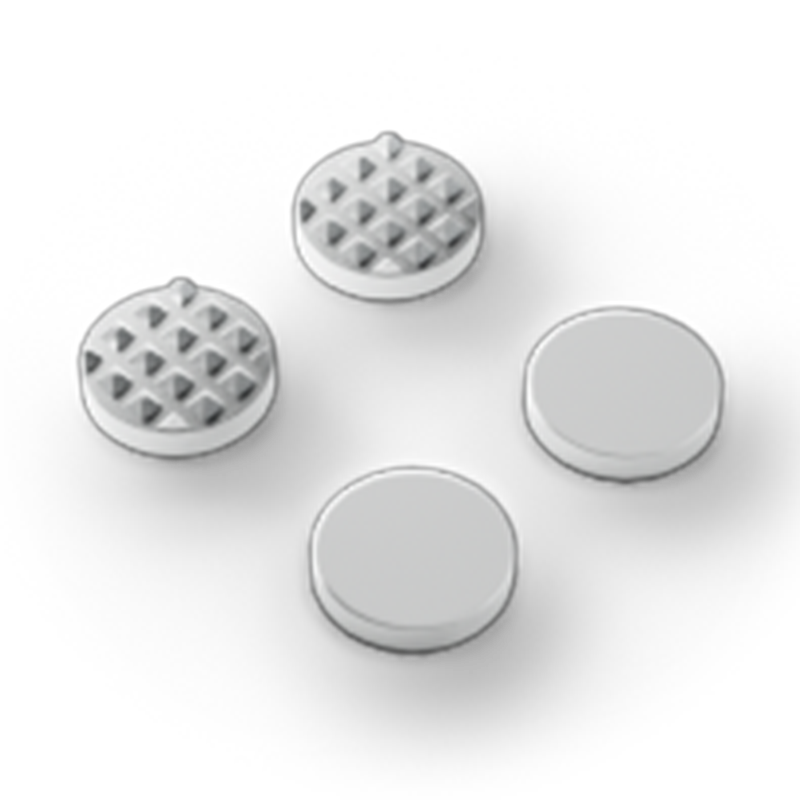
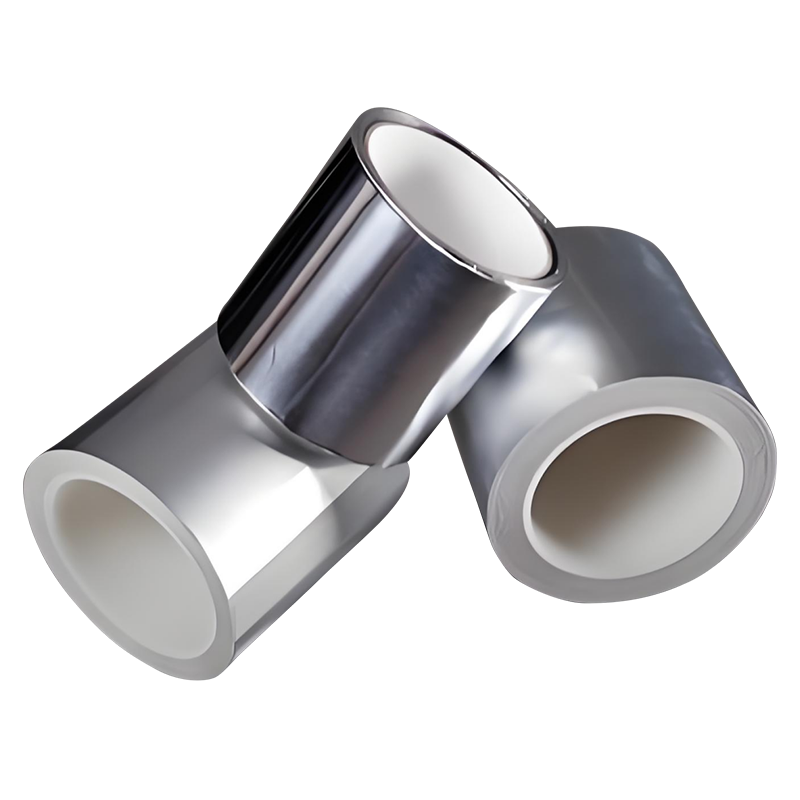
Surface treatment technologies also played a crucial role in enhancing the performance and longevity of IC lead frames. Techniques such as micro-etching, electroplating roughening, and brown oxidation were developed to improve adhesion between the lead frame and molding compounds while ensuring compatibility with various bonding materials like gold, aluminum, and copper wires. These treatments significantly boosted the moisture resistance and overall reliability of packaged ICs, helping many products achieve MSL.1 classification—a critical standard in harsh operating environments.
As semiconductor packaging continues to evolve toward system-in-package (SiP) and 3D integration, the IC lead frame remains a foundational element despite growing competition from substrate-based solutions. Its adaptability, cost-efficiency, and proven track record in mass production ensure its continued relevance across a wide range of industries—from consumer electronics and telecommunications to industrial automation and smart mobility solutions. At our facility, we continue to invest in next-generation lead frame manufacturing processes to stay ahead of these trends and deliver reliable, high-performance components tailored to tomorrow’s electronic needs.
Choosing the right IC lead frame is no longer just about basic connectivity—it's about enabling smarter, faster, and more durable electronic systems. With years of experience in designing and producing specialized lead frames for evolving packaging standards, we are committed to supporting innovation across the semiconductor supply chain. Whether you're developing cutting-edge IoT devices or robust automotive electronics, our lead frames are engineered to meet the highest levels of performance and reliability in real-world applications.
Copyright © Wenzhou Hongfeng Electrical Alloy Co., Ltd. All Rights Reserved. Metal Composite Materials Manufacturers
